The Heart of Electronics: A Comprehensive Guide to Printed Circuit Boards (PCBs)
Printed Circuit Boards (PCBs) are the silent heroes behind the gadgets we rely on daily. They are the fundamental building blocks of modern electronics, facilitating the interconnection of various electronic components in a neat and organized manner. In this article, we will take an in-depth journey into the world of PCBs, exploring their structure, functions, design considerations, manufacturing processes, and emerging trends. Check out full turnkey assembly to learn more.
Understanding PCBs
What is a PCB?
A Printed Circuit Board (PCB) is a flat, rigid board typically composed of non-conductive material (often fiberglass-reinforced epoxy) that serves as a foundation for connecting electronic components. PCBs provide mechanical support and a structured platform for components to be attached securely.
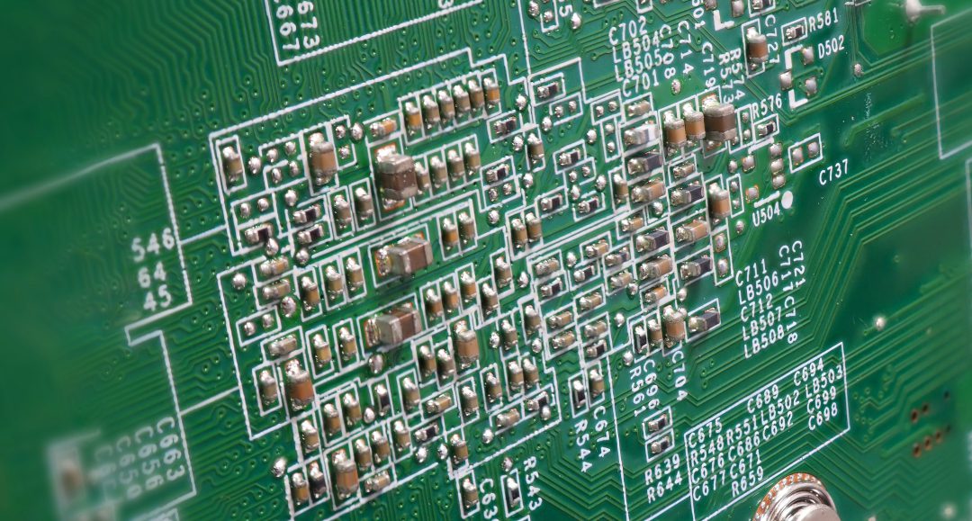
PCB Components and Layers
Substrate Layer: The primary material of a PCB, usually made of fiberglass-reinforced epoxy, provides the board's structural integrity.
Copper Traces: Thin layers of copper are etched onto the substrate, forming the conductive paths or traces that carry electrical signals between components.
Solder Mask: This protective layer covers the PCB's surface, with openings only where soldering is necessary. It prevents accidental solder bridges and safeguards copper traces from oxidation.
Silkscreen: Silkscreen printing is used to label components, provide reference designators, and add other information, such as logos or instructions, to the PCB's surface.
Components: Electronic components, including resistors, capacitors, integrated circuits, and connectors, are mounted onto the PCB. These components are soldered onto the copper traces to create electrical connections.
PCB Manufacturing Process
Design
The PCB design process begins with creating a schematic diagram, outlining component connections and placements. Specialized software, such as Eagle, Altium, or KiCad, is used for PCB layout and design.
Printing
Copper traces and other features are printed onto the substrate through photolithography. A mask is employed to selectively remove the copper layer, leaving behind the desired traces.
Etching
The PCB is submerged in an etchant, like ferric chloride, which eliminates exposed copper, leaving only the required traces and connections.
Drilling
Small holes, known as vias, are drilled into the PCB for connecting traces on different layers or mounting components. Automated drilling machines ensure precision.
Plating
Vias and exposed copper are plated with a thin layer of metal, often copper, to enhance conductivity and protect against corrosion.
Solder Mask Application
A solder mask is applied, covering the entire PCB surface except for areas where components will be soldered. This prevents solder bridges and preserves the integrity of copper traces.
Component Assembly
Components are placed on the PCB using automated pick-and-place machines. Solder paste is applied, and the board is sent through a reflow oven to melt the solder, creating secure electrical connections.
Inspection and Testing
Each PCB undergoes thorough inspection and testing to meet quality standards. Any defects or issues are identified and corrected.
Advancements in PCB Technology
The PCB industry continues to evolve, introducing innovative technologies and materials to meet the demands of smaller, more powerful, and energy-efficient electronics. Some noteworthy advancements include:
Miniaturization
Smaller components and finer trace widths allow for the development of compact and high-density PCBs, enabling the creation of smaller and more portable devices.
Flexible and Rigid-Flex PCBs
Flexible PCBs can be bent or twisted, making them ideal for applications like wearable technology. Rigid-flex PCBs combine the advantages of both rigid and flexible boards.
Advanced Materials
The use of advanced materials like ceramic PCBs, metal-core PCBs, and high-frequency laminates allows for better thermal management and performance in specialized applications.
3D Printing
Additive manufacturing techniques, such as 3D printing, are being explored for PCB prototyping, enabling rapid design iterations and reducing lead times.
Conclusion
Printed Circuit Boards are the unsung heroes of our digital age, enabling the seamless functioning of electronic devices we rely on daily. Understanding the intricacies of PCBs, from their components and manufacturing processes to emerging trends in technology, is essential for engineers, designers, and electronics enthusiasts as we continue to push the boundaries of what electronics can achieve in the future.